
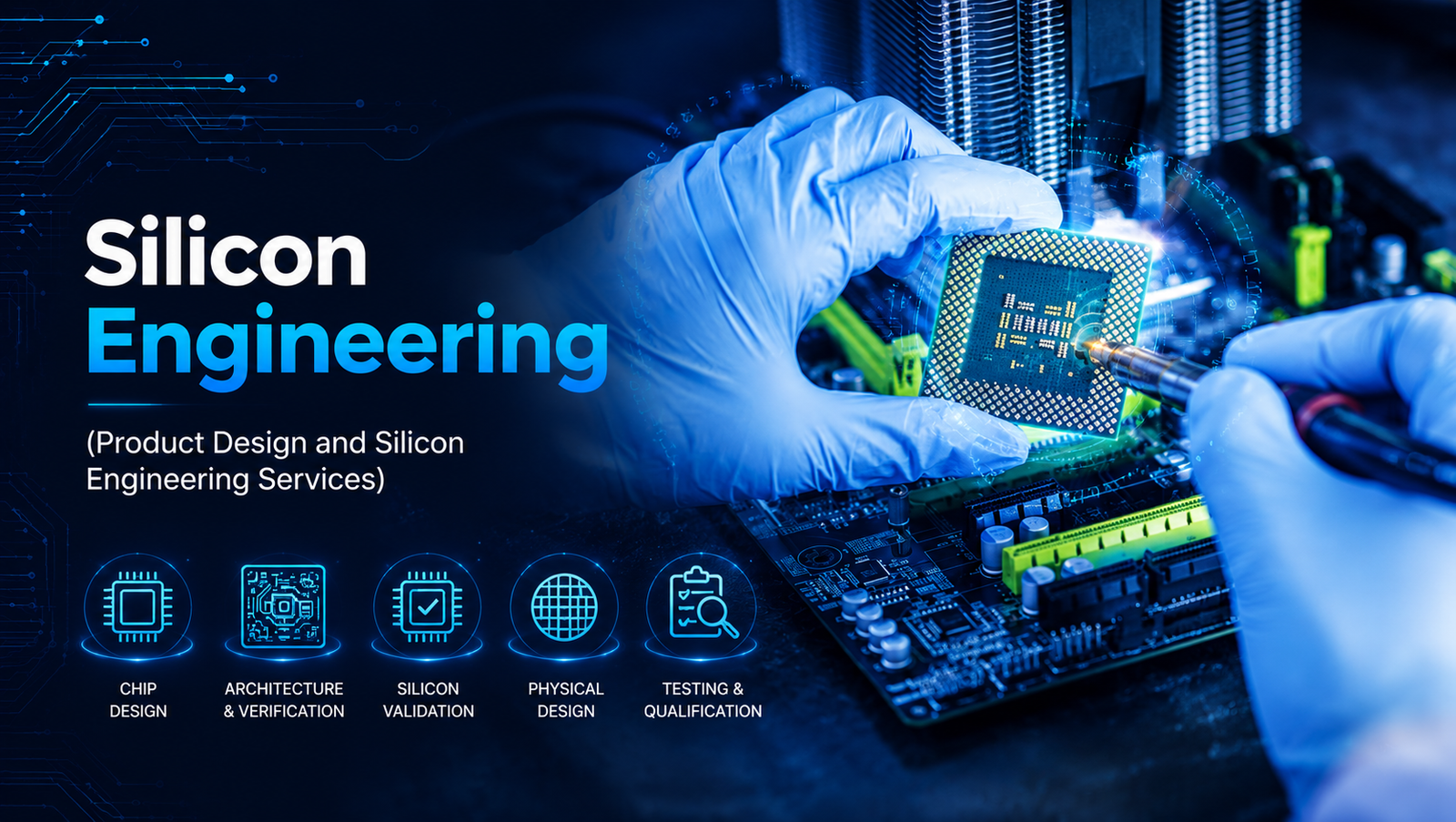
The world is rapidly moving towards an era of anywhere, anytime, and any-device computing. The semiconductor industry and embedded solution providers are driving this transformation by enabling the next generation of IoT-powered innovations. Growing demand for advanced technologies such as smartphones, tablets, electric vehicles, wearable devices, and smart electronics has significantly increased the need for high-performance microcontrollers, sensors, memory solutions, and next-generation semiconductor technologies.
At eInfochips, we provide end-to-end product design and silicon engineering services that help semiconductor companies accelerate innovation and reduce time-to-market. Our expertise spans VLSI chip design, Design for Testability (DFT), Design for Manufacturing (DFM), pre- and post-silicon validation, low-geometry design, and high-reliability on-chip solutions. With deep engineering expertise and proven methodologies, we enable clients to build robust, scalable, and future-ready semiconductor products.
End-to-end architecture and RTL design services for complex ASICs, FPGAs, and System-on-Chip (SoC) integration.
Comprehensive functional verification, UVM-based methodologies, and emulation to ensure first-pass silicon success.
Advanced node physical design, synthesis, timing closure, and Design-for-Testability (DFT) implementation.
Custom analog and mixed-signal block design, layout, and simulation for high-performance and low-power applications.
Complete silicon product realization from concept and specification through development to final GDSII delivery.
Cost-effective development of new product variants and generations based on existing silicon architectures.
Custom intellectual property blocks and verification IPs to accelerate SoC integration and time-to-market.
Hardware-accelerated emulation platforms for early software development and rigorous system-level validation.